Printed Circuit Boards (PCBs) are the core of modern electronics, forming the foundation of virtually every device we use. If you’ve ever wondered how these boards are brought to life, this guide walks you through the fundamental stages of PCB design. If you want to excel in this career path, then it is recommended that you upgrade your skills and knowledge regularly with the latestPCB Design Course in Bangalore.
What is PCB Design?
PCB design is the process of developing a physical layout that enables electronic components—such as resistors, capacitors, and integrated circuits—to work together efficiently. The aim is to create a functional and manufacturable board that meets both electrical and mechanical requirements.
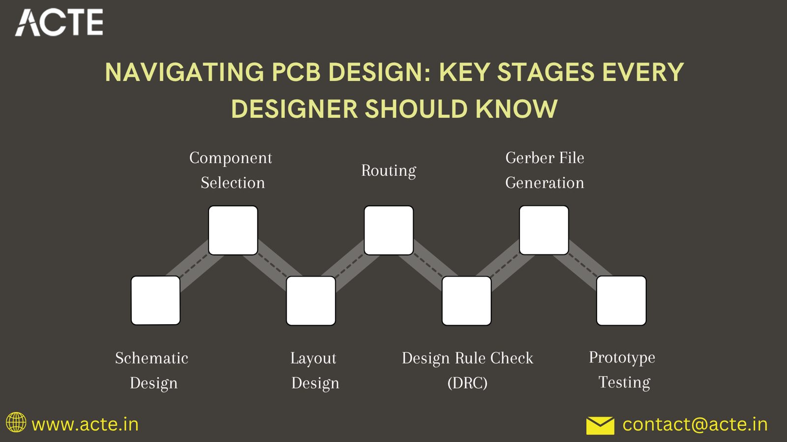
Key Stages in PCB Design
1. Schematic Design
Every PCB project begins with a schematic diagram—a visual plan detailing electrical connections between components. During this stage, designers:
Choose the necessary electronic components.
Position them logically based on circuit function.
Connect them using virtual wiring to create a complete electrical circuit.
2. Component Selection
Selecting the right parts determines the board’s performance and reliability. Important factors include:
Electrical ratings like voltage and current capacity.
Physical size and package type.
Cost, lead time, and availability.
3. Layout Design
After finalizing the schematic, the design transitions to the board layout. This involves:
Converting the circuit into a physical representation.
Placing components strategically to balance performance and space use.
Ensuring all parts fit within the defined board dimensions.
It’s simpler to master this tool and progress your profession with the help of PCB Design Training which provide thorough instruction and job placement support to anyone seeking to improve their talents.
4. Routing
Routing connects the placed components with copper traces. Effective routing considers:
Appropriate trace widths for current flow.
Short, efficient trace paths to minimize resistance.
Adequate spacing to prevent signal interference.
5. Design Rule Check (DRC)
Before manufacturing, a Design Rule Check ensures the layout meets all technical and fabrication requirements. This includes:
Detecting clearance and trace width issues.
Verifying that every component connection is correct.
6. Gerber File Generation
Once the design is verified, it’s exported into Gerber files—the standard format used by PCB manufacturers. These files specify:
Layer details.
Drill hole and via positions.
Component placements and copper traces.
7. Prototype Testing
The final stage is prototyping, where a sample board is fabricated and tested to confirm real-world functionality. This step helps to:
Reveal any unforeseen design flaws.
Ensure the circuit performs as intended.
Guide refinements before mass production.
Final Thoughts
Designing a PCB is a detailed process that blends creativity with engineering precision. By moving methodically through each stage—from schematic to prototype—you can produce boards that perform reliably and are ready for mass production. As electronics continue to evolve, gaining proficiency in PCB design and using modern design tools can greatly enhance your engineering toolkit.