Semiconductor Metrology and Inspection Market Size, Trends & Forecast Report 2033 | UnivDatos
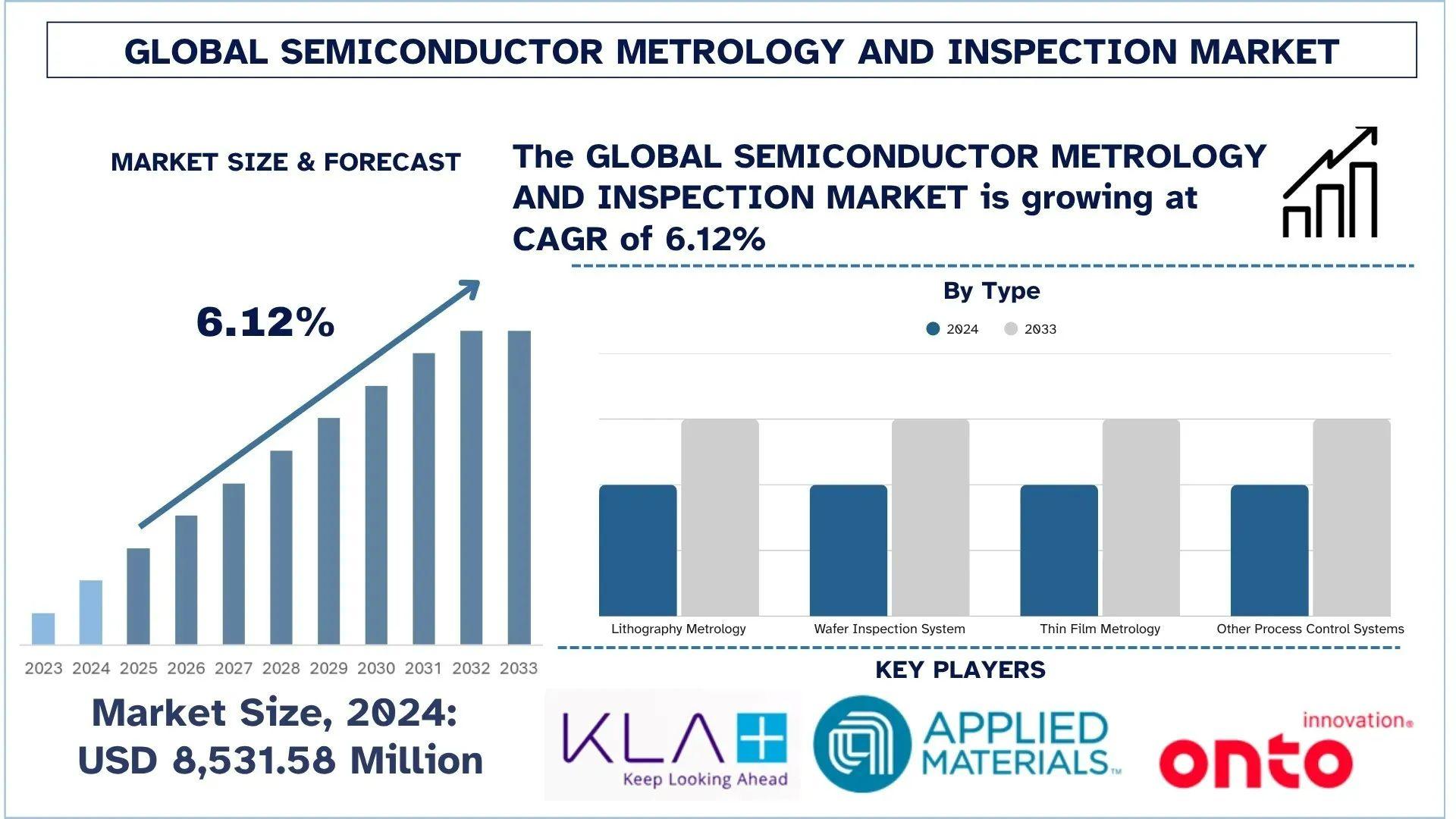
According to a new report by UnivDatos Market Insights, the Semiconductor Metrology and Inspection Market is expected to reach USD million in 2033 by growing at a CAGR of 6.12% during the forecast period (2025- 2033F).
The existing Semiconductor Metrology and Inspection market has a high growth rate due to an ever-increasing number of requirements for smaller, more powerful, and more efficient chips in sophisticated electronics, AI, and automotive markets. With nodes at or below 5nm, it becomes increasingly important to have accuracy in the detection of defects and the accuracy of the process. The need for reliable metrology and inspection products is related to the enhancement of the yield and control of the processes that have to be performed within the semiconductor fabrication cycle, starting with the sequence of inspection actions that establish patterns over the surface of the wafer and ending with the packaging of the semiconductor devices. Advanced alternatives to plasma inspection include optical metrology, advanced X-ray inspection, and e-beam inspection, which is gaining popularity as they have a high resolution capacity. On the other hand, additional advanced inspection equipment is needed with the increase in EUV lithography progression, 3D chip structures, and heterogeneous integration.
Access sample report (including graphs, charts, and figures): https://univdatos.com/reports/semiconductor-metrology-and-inspection-market?popup=report-enquiry
KLA Corporation
KLA Corporation, together with its subsidiaries, engages in the design, manufacture, and marketing of process control, process-enabling, and yield management solutions for the semiconductor and related electronics industries worldwide. It operates through three segments: Semiconductor Process Control; Specialty Semiconductor Process; and PCB and Component Inspection. The company offers inspection and review tools to identify, locate, characterize, review, and analyze defects on various surfaces of patterned and unpatterned wafers; metrology systems that are used to measure pattern dimensions, film thickness, film stress, layer-to-layer alignment, pattern placement, surface topography, and electro-optical properties for wafers; chemical process control equipment; wired and wireless sensor wafers and reticles; wafer defect inspection, review, and metrology systems; reticle inspection and metrology systems; and semiconductor software solutions that provide run-time process control, defect excursion identification, process corrections, and defect classification to accelerate yield learning rates and reduce production risk. It also provides etch, plasma dicing, deposition, and other wafer processing technologies and solutions for the semiconductor and microelectronics industry. In addition, the company offers direct imaging, inspection, optical shaping, inkjet and additive printing, UV laser drilling, and computer-aided manufacturing and engineering solutions for the PCB market; inspection and electrical testing systems to identify and classify defects, as well as systems to repair defects for the display market; and inspection and metrology systems for quality control and yield improvement in advanced and traditional semiconductor packaging markets. The company was formerly known as KLA-Tencor Corporation and changed its name to KLA Corporation in July 2019. KLA Corporation was incorporated in 1975 and is headquartered in Milpitas, California.
|
Founded |
1975 |
|
Headquarter |
California, United States |
|
Employees |
15,115 |
|
Revenue (2024) |
USD 9,812.25 Million |
Applied Materials, Inc.
Applied Materials, Inc. engages in the provision of manufacturing equipment, services, and software to the semiconductor, display, and related industries. The company operates through three segments: Semiconductor Systems, Applied Global Services, and Display. The Semiconductor Systems segment develops, manufactures, and sells semiconductor capital equipment that is used to fabricate semiconductor chips or integrated circuits. The Applied Global Services segment provides integrated solutions to optimize equipment and fab performance and productivity comprising spares, upgrades, services, and other equipment and factory automation software for semiconductor, display, and other products. The Display segment offers products for manufacturing liquid crystal displays; organic light-emitting diodes; and other display technologies for TVs, monitors, laptops, personal computers, smart phones, and other consumer-oriented devices and solar energy cells. It focused on device innovations for chipmakers serving ICAPS markets. The company operates in the United States, China, Korea, Taiwan, Japan, Southeast Asia, Europe, and internationally. Applied Materials, Inc. was incorporated in 1967 and is headquartered in Santa Clara, California.
|
Founded |
1967 |
|
Headquarter |
California, United States |
|
Employees |
35,700 |
|
Revenue (2024) |
USD 27,176 Million |
Onto Innovation
Onto Innovation Inc. engages in the design, development, manufacture, and support of process control tools that performs optical metrology and inspection worldwide. The company offers lithography systems and process control analytical software. It also provides process and yield management solutions, and device packaging and test facilities through standalone systems for optical metrology, macro-defect inspection, packaging lithography, and transparent and opaque thin film measurements. In addition, the company offers process control software portfolio that includes solutions for standalone tools, groups of tools, and enterprise-or factory-wide suites. Further, it engages in systems and software, spare parts, and other services, as well as offers software licensing services. The company’s products are used in semiconductor and advanced packaging device manufacturers; silicon wafers; light emitting diodes; vertical-cavity surface-emitting lasers; micro-electromechanical systems; CMOS image sensors; power devices; analog devices; RF filters; data storage; and various industrial and scientific applications. Onto Innovation Inc. was founded in 1940 and is headquartered in Wilmington, Massachusetts.
|
Founded |
1940 |
|
Headquarter |
Massachusetts, United States |
|
Employees |
1,551 |
|
Revenue (2024) |
USD 987.32 Million |
Thermo Fisher Scientific Inc.
provides life sciences solutions, analytical instruments, specialty diagnostics, and laboratory products and biopharma services in the North America, Europe, Asia-Pacific, and internationally. The company’s Life Sciences Solutions segment offers reagents, instruments, and consumables for biological and medical research, discovery and production of drugs and vaccines, as well as diagnosis of infections and diseases. Its Analytical Instruments segment provides instruments, consumables, software, and services for pharmaceutical, biotechnology, academic, government, environmental, and other research and industrial markets, as well as clinical laboratories. The company’s Specialty Diagnostics segment includes clinical diagnostics offering liquid, ready-to-use, and lyophilized immunodiagnostic reagent kits, as well as calibrators, controls, protein detection assays, and instruments; immunodiagnostics offers develops, manufactures, and markets complete blood test systems to support the clinical diagnosis and monitoring of allergy, asthma, and autoimmune diseases; microbiology offers dehydrated and prepared culture media, collection and transport systems, instrumentation, and consumables; transplant diagnostics products include human leukocyte antigen typing and testing for organ transplant market; and healthcare market channel offers consumables, diagnostic kits and reagents, equipment, instruments, solutions, and services. Its Laboratory Products and Biopharma Services segment provides laboratory products, research and safety market channel, and pharma services and clinical research. It offers products and services through a direct sales force, customer-service professionals, electronic commerce, and third-party distributors under Thermo Scientific; Applied Biosystems; Invitrogen; Fisher Scientific; Unity Lab Services; and Patheon and PPD. Thermo Fisher Scientific Inc. was founded in 1956 and is headquartered in Waltham, Massachusetts.
|
Founded |
1956 |
|
Headquarter |
Massachusetts, United States |
|
Employees |
1,25,000 |
|
Revenue (2024) |
USD 42,879 Million |
Click here to view the Report Description & TOC https://univdatos.com/reports/semiconductor-metrology-and-inspection-market
Hitachi, Ltd.
Hitachi, Ltd. provides digital systems and services, green energy and mobility, and connective industry solutions in Japan and internationally. It operates through Digital Systems & Services, Green Energy & Mobility, Connective Industries, Automotive Systems, and other segments. The company offers system integration, consulting, cloud services, storage, servers, software, and ATMs; finance solutions, social infrastructure information systems, public IT solutions, IoT/data utilization, control systems, and cloud services; and IT products. It also provides power grids, clean, nuclear, renewable energy, and railway systems, such as urban railway signal and traffic control system, signaling and traffic control systems, freight rail signaling and traffic control system, ticketing and fare collection systems, and digital asset management; and elevators and escalators, home appliances, air conditioners, industry and distribution solution, water and environment solutions, and industrial machinery. In addition, the company offers semiconductor manufacturing equipment, clinical analyzers, electron and probe microscopes, powertrains, chassis, advanced driver assistance systems, and motorcycle systems, as well as property management and other services. Hitachi, Ltd. was founded in 1910 and is headquartered in Tokyo, Japan.
|
Founded |
1910 |
|
Headquarter |
Tokyo, Japan |
|
Employees |
2,82,743 |
|
Revenue (2024) |
USD 65,332.23 Million |
The rising demand for more minor, more powerful, and energy-efficient chips, particularly in advanced electronics, AI, and automotive sectors, is expected to drive the semiconductor metrology and inspection market.
Related Report :-
India Semiconductor Market: Current Analysis and Forecast (2024-2032)
EV Semiconductor Market: Current Analysis and Forecast (2022-2030)
Contact Us:
UnivDatos
Contact Number - +1 978 733 0253
Email - [email protected]
Website - www.univdatos.com
Linkedin- https://www.linkedin.com/company/univ-datos-market-insight/mycompany/